The flow of current through the conducting region controlled by an electric field. Hence the name field effect transistor (FET).
Table of Contents
FIELD EFFECT TRANSISTORS
FET (field effect transistor) is said to be a unipolar device because current conduction is only by majority carriers.
FET is a Voltage controlled device because its output characteristics are determined by the field which depends on the voltage applied.
It has three terminals named as
- Source (S)
- Drain(D)
- Gate(G)
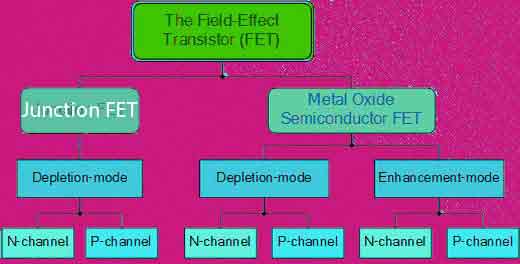
CLASSIFICATION OF FET
FET is classified into two types as follows,
*JFET (junction field-effect transistor).
1. n-channel
2.p-channel
*MOSFET(Metal Oxide Semiconductor (or) Insulated Gate FET.
>Depletion type
1.n-channel
2. p-channel
> Enhancement type
1.n-channel
2. p-channel
Advantages of JFET over BJT
- Operation depends upon the flowing of majority carriers only
- It exhibits a high input resistance (mega ohm) because gate constitutes no current but in BJT, base constitutes a current.
- Less noisy.
- It has thermal stability
Disadvantages in JFET
1.Small gain-bandwidth product.
JFET [ Junction Field Effect Transistor ]
- JFET may be used as a linear Resistor ≈ 0
- The drain current is controlled by a gate voltage applied at the gate VGSand IG~0
Therefore it is termed as “ voltage-controlled device”.
Types
1) N-channel JFET
2) P-channel JFET
Symbol

Construction

It consists of an N-type or P-type base which is made of silicon.
- Ohmic contacts made at the two ends of the base called source and drain.
Source(S):-
- Connected to the negative pole of the battery.
- Electrons enter the basis through this terminal for N-channel JFET.
Drain(D):-
- Connected to the positive pole of a battery.
- Electrons leave the basis through this terminal for N-channel JFET.
Gate(G):-
- Heavily doped P-type silicon is diffused on both sides of the N-channel basis by which PN junction are formed.
- These layers are joined together and called the gate.
Channel:-
- It is the space between the gate through which majority carriers pass.
Define FET?
A field-effect transistor (FET) is a three-terminal semiconductor instrument which can be used as an amplifier or switch. The 3 terminals are Drain (D), Source (S), and Gate (G).
Define channel?
It is a bar-like structure which fix the type of FET. Different types of N channel are FET and P channel FET.
Draw the transfer characteristic for n-channel depletion type MOSFET?
Transfer Characteristics:

>WHAT DO YOU UNDERSTAND BY PINCH-OFF VOLTAGE AND THE OUT OF VOLTAGE?
As the reverse bias is more increased, the effective width of the channel decreases, the depletion region or the space charge region widens, reaching more into the channel and restricting the crossing of electrons from the source to drain. Finally at a certain gate to source voltage VGS = VP.
Why FET is called as “voltage-operated device”?
In FET the output current, I D is controlled by the voltage applied between gate and source (VGS). Therefore FET is said to be a voltage-controlled device.
Which, MOSFET is called Normally ON MOSFET and NORMALLY OFF MOSFET? Why?
This is only one type of MOSFET, called ‘normally -off’ because it is only the application of a positive gate voltage above the tight voltage which permits it to pass current between the source and drains. Another type of MOSFET is the ‘normally-on’, which has a conductive channel of less heavily doped n-type material between the source and drain electrodes.
COMPARE BJT AND MOSFET?

BJT
1 CB,CE,CC configurations
2 Less input resistance compared to JFET
3 Input-output relation is linear
4 Gain bandwidth product is high
5 Thermal noise is more
6 Thermal stability is less
7 Bigger size than MOSFET
MOSFET
1CG, CS,CD configurations
2 Very high input resistance
3 Input-output relation is non-linear
4 Gain bandwidth product is low
5 Thermal noise is less
6 Thermal stability is more
7 Smaller size
Comparison between JFET and BJT?

BJT
1 Low input impedance
2 High output impedance
3 Bipolar device
4 Noise is more
5 Cheaper
6 Gain is more
7 Current controlled device
JFET
1 High input impedance
2 Low output impedance
3 Unipolar device
4 Less noise
5 Costlier
6 Less gain
7 Voltage-controlled device
What are the important features of FET?
- The parameters of FET(Field-effect Transistor) are temperature-dependent. In FET, as temperature increases drain resistance further increases, reducing the drain current. Thus unlike BJT, thermal runaway doesn’t occur with FET. Thus we can say FET(Field-effect Transistor) is more temperature stable.
- FET has a very high input impedance. Hence, FET is preferred in amplifiers. It’s less noisy.
- Requires less space.
- It exhibits no offset voltage at zero drains current D.
Comparison between JFET and MOSFET?

JFET
1 Operated in depletion mode
2 High input impedance(>10MΩ)
3 Gate is not insulated from the channel
4 Channel exists permanently
5 Difficult to fabricate than MOSFET
6 Drain resistance is high
7 Gate is formed as a diode
MOSFET
1 Operated in depletion mode and enhancement mode
2 Very high input impedance(>10000MΩ)
3 Gate is insulated from the channel by a layer of Sio2
4 Channel exists abidingly in depletion type but not in enhancement type.
5 Easier to fabricate
6 Drain resistance is less
7 Gate is formed as a capacitor
Write the advantages of JFET?
The input impedance of JFET is very high.
This allows a high degree of Isolation between the Input and Output circuit. The current bearer isn’t crossing the junction hence noise is reduced drastically.
Explain the depletion node of operation in MOSFET?
When the gate is a negative bias, the thickness of the depletion layer further increases owing to the further increase of the induced positive charge. Thus, the drain current decreases, as the gate is built more negative. This is called the depletion mode of operation.
Explain the term Drain in FET?
The drain is the terminal per which the current leaves the bar. Convention current ingoing the bar is designated as ID.
Define the term Gate in FET?
The gate consists of either P+ or N+ impurity regions, heavily doped and diffused to the bar. This region is permanently reverse biased and in fact, controls the drain current ID.
Write the relative disadvantages of a FET over that of a BJT?
*The gain-bandwidth product in case of a FET(Field-Effect Transistor) is low as compared with a BJT.
*The class, called MOSFET, is extremely sensitive to handling, therefore, additional precautions have to be considered while handling.
Why MOSFET is called IGFET?
MOSFET is constructed with a gate terminal insulated from the channel. So it is also called as insulated gate FET(Field-Effect Transistor) or IGFET.
Compare P channel and N channel JFET?

N- channel JFET
1 Current carriers are electrons
2 Mobility of electrons is almost double bond that of holes in p-channel
3 Low input noise
4 Transconductance is very high
P-channel JFET
1 Current carriers are holes
2 Mobility of holes is poor
3 Large input noise
4 Transconductance is very small
INDUCTION MOTOR | WHY DOES THE ROTOR ROTATE | WORKING PRINCIPLE
WORKING PRINCIPLE OF ALTERNATOR
SPEED CONTROL OF DC MOTOR (SHUNT, SERIES, AND COMPOUND)
SPEED TORQUE CHARACTERISTICS OF D.C MOTOR
Wye Delta Transformation | Diagram & Formula | Application
Semiconductor Diode/Types of Diode/And Their Application
Owner Of ICEEET


8 comments
I just like the helpful info you supply to your articles. I’ll bookmark your blog and check again here regularly. I’m moderately certain I will be informed plenty of new stuff proper here! Good luck for the next!| а
Thanks
Kitap Sitelerinin Adları Şu An En Çok Okunan Kitaplar
[…] of transistor, it works as long as the light falls on it. The light acts as the base pin of the transistor. It acts like a switch when the current flows when the light is on, but not in the […]
[…] into digital. So what are the analog tasks? Analog work is meant to work on various types of IC, transistor diode and so on. The microcontroller can work on all of these devices simultaneously with a digital […]
[…] that can control electron flow and current flow by themselves are called active devices. Such as BJT, JFET, MOSFET, […]
Good day! Do you know if they make any plugins to assist with Search Engine Optimization? I’m trying to get my blog to rank for some targeted keywords but I’m not seeing very good results. If you know of any please share. Kudos!|
I used Yoast SEO Premium Plugin